1. Product Features and Structural Integrity
1.1 Intrinsic Features of Silicon Carbide
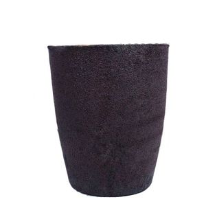
(Silicon Carbide Crucibles)
Silicon carbide (SiC) is a covalent ceramic compound made up of silicon and carbon atoms set up in a tetrahedral latticework structure, primarily existing in over 250 polytypic kinds, with 6H, 4H, and 3C being the most technologically appropriate.
Its solid directional bonding conveys exceptional hardness (Mohs ~ 9.5), high thermal conductivity (80– 120 W/(m · K )for pure single crystals), and exceptional chemical inertness, making it among one of the most robust products for severe environments.
The vast bandgap (2.9– 3.3 eV) ensures exceptional electrical insulation at room temperature level and high resistance to radiation damage, while its low thermal expansion coefficient (~ 4.0 × 10 ⁻⁶/ K) contributes to remarkable thermal shock resistance.
These intrinsic properties are maintained also at temperatures surpassing 1600 ° C, allowing SiC to keep structural honesty under long term direct exposure to thaw metals, slags, and reactive gases.
Unlike oxide ceramics such as alumina, SiC does not respond conveniently with carbon or form low-melting eutectics in lowering ambiences, a crucial benefit in metallurgical and semiconductor processing.
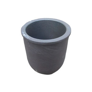
When made into crucibles– vessels created to consist of and warmth products– SiC outperforms traditional products like quartz, graphite, and alumina in both lifespan and procedure integrity.
1.2 Microstructure and Mechanical Security
The performance of SiC crucibles is closely tied to their microstructure, which relies on the manufacturing technique and sintering additives made use of.
Refractory-grade crucibles are normally created through reaction bonding, where permeable carbon preforms are penetrated with molten silicon, creating β-SiC through the response Si(l) + C(s) → SiC(s).
This process yields a composite framework of primary SiC with recurring free silicon (5– 10%), which improves thermal conductivity but may limit usage over 1414 ° C(the melting factor of silicon).
Conversely, totally sintered SiC crucibles are made through solid-state or liquid-phase sintering utilizing boron and carbon or alumina-yttria ingredients, achieving near-theoretical density and higher pureness.
These display superior creep resistance and oxidation security but are much more pricey and difficult to fabricate in plus sizes.
( Silicon Carbide Crucibles)
The fine-grained, interlacing microstructure of sintered SiC provides excellent resistance to thermal fatigue and mechanical erosion, important when managing molten silicon, germanium, or III-V compounds in crystal development procedures.
Grain limit design, consisting of the control of secondary stages and porosity, plays an important role in identifying long-lasting sturdiness under cyclic home heating and hostile chemical atmospheres.
2. Thermal Efficiency and Environmental Resistance
2.1 Thermal Conductivity and Heat Circulation
Among the defining benefits of SiC crucibles is their high thermal conductivity, which makes it possible for fast and uniform warm transfer throughout high-temperature processing.
Unlike low-conductivity materials like integrated silica (1– 2 W/(m · K)), SiC successfully distributes thermal power throughout the crucible wall, lessening local hot spots and thermal slopes.
This uniformity is important in processes such as directional solidification of multicrystalline silicon for photovoltaics, where temperature level homogeneity directly affects crystal high quality and problem density.
The mix of high conductivity and low thermal development results in an exceptionally high thermal shock parameter (R = k(1 − ν)α/ σ), making SiC crucibles immune to fracturing throughout rapid home heating or cooling cycles.
This permits faster heating system ramp prices, improved throughput, and lowered downtime due to crucible failing.
Additionally, the product’s capacity to hold up against duplicated thermal biking without considerable degradation makes it ideal for batch processing in industrial heaters running above 1500 ° C.
2.2 Oxidation and Chemical Compatibility
At raised temperatures in air, SiC undertakes easy oxidation, forming a protective layer of amorphous silica (SiO TWO) on its surface: SiC + 3/2 O TWO → SiO TWO + CO.
This glassy layer densifies at heats, functioning as a diffusion barrier that slows down additional oxidation and preserves the underlying ceramic framework.
Nonetheless, in reducing ambiences or vacuum cleaner conditions– typical in semiconductor and metal refining– oxidation is subdued, and SiC remains chemically stable against molten silicon, aluminum, and many slags.
It stands up to dissolution and reaction with molten silicon up to 1410 ° C, although extended direct exposure can bring about small carbon pick-up or user interface roughening.
Crucially, SiC does not present metal pollutants right into sensitive melts, a vital demand for electronic-grade silicon production where contamination by Fe, Cu, or Cr should be maintained below ppb degrees.
However, treatment needs to be taken when refining alkaline earth steels or very responsive oxides, as some can wear away SiC at extreme temperature levels.
3. Manufacturing Processes and Quality Control
3.1 Construction Strategies and Dimensional Control
The production of SiC crucibles involves shaping, drying, and high-temperature sintering or infiltration, with techniques selected based on required pureness, size, and application.
Typical creating techniques consist of isostatic pushing, extrusion, and slip spreading, each supplying different levels of dimensional precision and microstructural harmony.
For big crucibles used in solar ingot spreading, isostatic pressing makes sure consistent wall thickness and density, lowering the risk of asymmetric thermal expansion and failure.
Reaction-bonded SiC (RBSC) crucibles are affordable and extensively used in factories and solar markets, though recurring silicon limitations optimal service temperature.
Sintered SiC (SSiC) versions, while much more expensive, offer premium pureness, toughness, and resistance to chemical assault, making them ideal for high-value applications like GaAs or InP crystal growth.
Precision machining after sintering might be called for to attain limited resistances, specifically for crucibles made use of in upright slope freeze (VGF) or Czochralski (CZ) systems.
Surface completing is critical to decrease nucleation websites for problems and make sure smooth thaw circulation throughout spreading.
3.2 Quality Assurance and Efficiency Recognition
Strenuous quality assurance is essential to ensure integrity and long life of SiC crucibles under requiring operational problems.
Non-destructive evaluation strategies such as ultrasonic screening and X-ray tomography are employed to identify interior splits, gaps, or density variations.
Chemical evaluation through XRF or ICP-MS validates reduced levels of metallic contaminations, while thermal conductivity and flexural toughness are determined to verify material uniformity.
Crucibles are frequently subjected to simulated thermal cycling examinations before shipment to identify potential failing settings.
Batch traceability and accreditation are conventional in semiconductor and aerospace supply chains, where element failure can lead to expensive production losses.
4. Applications and Technical Impact
4.1 Semiconductor and Photovoltaic Industries
Silicon carbide crucibles play a pivotal role in the manufacturing of high-purity silicon for both microelectronics and solar cells.
In directional solidification heaters for multicrystalline photovoltaic or pv ingots, big SiC crucibles act as the key container for molten silicon, enduring temperature levels above 1500 ° C for numerous cycles.
Their chemical inertness prevents contamination, while their thermal security guarantees uniform solidification fronts, bring about higher-quality wafers with fewer dislocations and grain borders.
Some suppliers layer the inner surface area with silicon nitride or silica to further decrease adhesion and promote ingot release after cooling down.
In research-scale Czochralski development of compound semiconductors, smaller sized SiC crucibles are used to hold melts of GaAs, InSb, or CdTe, where marginal sensitivity and dimensional security are critical.
4.2 Metallurgy, Shop, and Arising Technologies
Beyond semiconductors, SiC crucibles are important in steel refining, alloy preparation, and laboratory-scale melting procedures involving light weight aluminum, copper, and rare-earth elements.
Their resistance to thermal shock and erosion makes them excellent for induction and resistance heating systems in foundries, where they outlive graphite and alumina alternatives by numerous cycles.
In additive production of responsive metals, SiC containers are used in vacuum induction melting to stop crucible malfunction and contamination.
Emerging applications include molten salt activators and focused solar energy systems, where SiC vessels might consist of high-temperature salts or fluid metals for thermal energy storage space.
With recurring advances in sintering technology and finishing design, SiC crucibles are positioned to sustain next-generation materials handling, allowing cleaner, much more efficient, and scalable industrial thermal systems.
In recap, silicon carbide crucibles represent a vital enabling modern technology in high-temperature material synthesis, combining phenomenal thermal, mechanical, and chemical performance in a solitary engineered part.
Their prevalent fostering throughout semiconductor, solar, and metallurgical markets highlights their duty as a cornerstone of modern-day commercial ceramics.
5. Provider
Advanced Ceramics founded on October 17, 2012, is a high-tech enterprise committed to the research and development, production, processing, sales and technical services of ceramic relative materials and products. Our products includes but not limited to Boron Carbide Ceramic Products, Boron Nitride Ceramic Products, Silicon Carbide Ceramic Products, Silicon Nitride Ceramic Products, Zirconium Dioxide Ceramic Products, etc. If you are interested, please feel free to contact us.
Tags: Silicon Carbide Crucibles, Silicon Carbide Ceramic, Silicon Carbide Ceramic Crucibles
All articles and pictures are from the Internet. If there are any copyright issues, please contact us in time to delete.
Inquiry us