1. Product Basics and Architectural Features of Alumina Ceramics
1.1 Crystallographic and Compositional Basis of α-Alumina
(Alumina Ceramic Substrates)
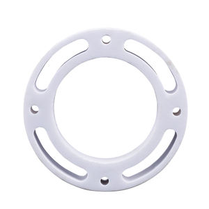
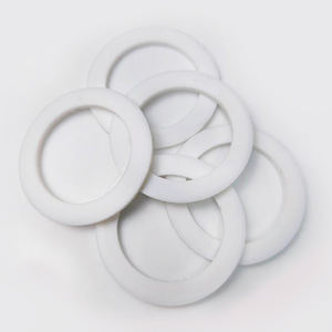
Alumina ceramic substratums, largely composed of light weight aluminum oxide (Al two O FIVE), function as the foundation of contemporary digital packaging because of their extraordinary balance of electrical insulation, thermal stability, mechanical stamina, and manufacturability.
The most thermodynamically stable phase of alumina at heats is corundum, or α-Al Two O TWO, which crystallizes in a hexagonal close-packed oxygen lattice with light weight aluminum ions occupying two-thirds of the octahedral interstitial websites.
This thick atomic plan conveys high firmness (Mohs 9), outstanding wear resistance, and solid chemical inertness, making α-alumina appropriate for rough operating atmospheres.
Commercial substrates typically have 90– 99.8% Al Two O FIVE, with minor additions of silica (SiO ₂), magnesia (MgO), or uncommon earth oxides made use of as sintering aids to advertise densification and control grain growth throughout high-temperature processing.
Higher purity grades (e.g., 99.5% and over) display premium electric resistivity and thermal conductivity, while lower pureness variants (90– 96%) supply cost-efficient remedies for much less demanding applications.
1.2 Microstructure and Defect Design for Electronic Dependability
The performance of alumina substratums in electronic systems is seriously depending on microstructural uniformity and problem minimization.
A penalty, equiaxed grain framework– commonly ranging from 1 to 10 micrometers– ensures mechanical honesty and decreases the probability of crack propagation under thermal or mechanical stress and anxiety.
Porosity, especially interconnected or surface-connected pores, must be decreased as it deteriorates both mechanical toughness and dielectric performance.
Advanced processing methods such as tape casting, isostatic pushing, and regulated sintering in air or managed atmospheres allow the production of substratums with near-theoretical density (> 99.5%) and surface roughness listed below 0.5 µm, crucial for thin-film metallization and cable bonding.
In addition, contamination partition at grain limits can result in leak currents or electrochemical movement under prejudice, necessitating stringent control over basic material pureness and sintering problems to ensure long-lasting dependability in damp or high-voltage atmospheres.
2. Manufacturing Processes and Substratum Manufacture Technologies
( Alumina Ceramic Substrates)
2.1 Tape Spreading and Environment-friendly Body Handling
The production of alumina ceramic substrates begins with the preparation of an extremely dispersed slurry containing submicron Al two O four powder, natural binders, plasticizers, dispersants, and solvents.
This slurry is processed via tape spreading– a continual method where the suspension is topped a relocating carrier movie making use of a precision medical professional blade to achieve consistent density, usually between 0.1 mm and 1.0 mm.
After solvent dissipation, the resulting “eco-friendly tape” is adaptable and can be punched, drilled, or laser-cut to form using openings for vertical affiliations.
Numerous layers may be laminated to create multilayer substratums for intricate circuit integration, although most of industrial applications utilize single-layer arrangements because of cost and thermal growth factors to consider.
The eco-friendly tapes are after that carefully debound to remove organic additives via controlled thermal decay before final sintering.
2.2 Sintering and Metallization for Circuit Integration
Sintering is conducted in air at temperature levels between 1550 ° C and 1650 ° C, where solid-state diffusion drives pore elimination and grain coarsening to accomplish full densification.
The straight shrinkage throughout sintering– commonly 15– 20%– should be specifically forecasted and made up for in the style of eco-friendly tapes to guarantee dimensional precision of the last substratum.
Complying with sintering, metallization is applied to form conductive traces, pads, and vias.
Two primary methods dominate: thick-film printing and thin-film deposition.
In thick-film technology, pastes consisting of metal powders (e.g., tungsten, molybdenum, or silver-palladium alloys) are screen-printed onto the substratum and co-fired in a decreasing ambience to develop durable, high-adhesion conductors.
For high-density or high-frequency applications, thin-film processes such as sputtering or dissipation are used to down payment adhesion layers (e.g., titanium or chromium) complied with by copper or gold, allowing sub-micron pattern using photolithography.
Vias are full of conductive pastes and discharged to develop electric interconnections between layers in multilayer layouts.
3. Practical Features and Efficiency Metrics in Electronic Solution
3.1 Thermal and Electrical Behavior Under Functional Anxiety
Alumina substrates are treasured for their positive mix of modest thermal conductivity (20– 35 W/m · K for 96– 99.8% Al Two O FOUR), which enables reliable warmth dissipation from power gadgets, and high volume resistivity (> 10 ¹⁴ Ω · cm), ensuring marginal leak current.
Their dielectric constant (εᵣ ≈ 9– 10 at 1 MHz) is stable over a broad temperature level and regularity range, making them ideal for high-frequency circuits up to several gigahertz, although lower-κ products like aluminum nitride are liked for mm-wave applications.
The coefficient of thermal growth (CTE) of alumina (~ 6.8– 7.2 ppm/K) is reasonably well-matched to that of silicon (~ 3 ppm/K) and specific product packaging alloys, minimizing thermo-mechanical tension during tool operation and thermal biking.
Nevertheless, the CTE inequality with silicon stays a worry in flip-chip and straight die-attach arrangements, often requiring certified interposers or underfill materials to mitigate fatigue failure.
3.2 Mechanical Robustness and Environmental Longevity
Mechanically, alumina substrates show high flexural strength (300– 400 MPa) and excellent dimensional stability under lots, allowing their use in ruggedized electronics for aerospace, automobile, and commercial control systems.
They are resistant to vibration, shock, and creep at elevated temperature levels, maintaining structural stability as much as 1500 ° C in inert environments.
In moist environments, high-purity alumina reveals minimal moisture absorption and outstanding resistance to ion migration, ensuring lasting integrity in exterior and high-humidity applications.
Surface area firmness likewise shields against mechanical damages throughout handling and assembly, although care needs to be taken to avoid side damaging due to fundamental brittleness.
4. Industrial Applications and Technical Influence Throughout Sectors
4.1 Power Electronic Devices, RF Modules, and Automotive Solutions
Alumina ceramic substrates are common in power digital modules, including shielded gateway bipolar transistors (IGBTs), MOSFETs, and rectifiers, where they offer electric isolation while facilitating heat transfer to heat sinks.
In superhigh frequency (RF) and microwave circuits, they function as provider systems for crossbreed integrated circuits (HICs), surface acoustic wave (SAW) filters, and antenna feed networks as a result of their secure dielectric homes and low loss tangent.
In the auto industry, alumina substratums are used in engine control systems (ECUs), sensor packages, and electrical automobile (EV) power converters, where they sustain heats, thermal biking, and exposure to harsh liquids.
Their integrity under extreme problems makes them important for safety-critical systems such as anti-lock braking (ABDOMINAL MUSCLE) and advanced motorist aid systems (ADAS).
4.2 Clinical Devices, Aerospace, and Arising Micro-Electro-Mechanical Systems
Past customer and industrial electronics, alumina substratums are utilized in implantable medical gadgets such as pacemakers and neurostimulators, where hermetic sealing and biocompatibility are paramount.
In aerospace and defense, they are used in avionics, radar systems, and satellite interaction modules as a result of their radiation resistance and security in vacuum cleaner atmospheres.
Furthermore, alumina is progressively utilized as a structural and insulating platform in micro-electro-mechanical systems (MEMS), including stress sensors, accelerometers, and microfluidic tools, where its chemical inertness and compatibility with thin-film handling are useful.
As electronic systems remain to demand greater power densities, miniaturization, and dependability under severe problems, alumina ceramic substratums stay a keystone material, linking the void between efficiency, cost, and manufacturability in innovative electronic packaging.
5. Provider
Alumina Technology Co., Ltd focus on the research and development, production and sales of aluminum oxide powder, aluminum oxide products, aluminum oxide crucible, etc., serving the electronics, ceramics, chemical and other industries. Since its establishment in 2005, the company has been committed to providing customers with the best products and services. If you are looking for high quality porous alumina, please feel free to contact us. (nanotrun@yahoo.com)
Tags: Alumina Ceramic Substrates, Alumina Ceramics, alumina
All articles and pictures are from the Internet. If there are any copyright issues, please contact us in time to delete.
Inquiry us