1. Material Scientific Research and Structural Characteristic
1.1 Crystal Framework and Chemical Security
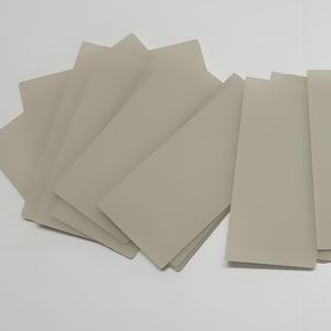
(Aluminum Nitride Ceramic Substrates)
Aluminum nitride (AlN) is a broad bandgap semiconductor ceramic with a hexagonal wurtzite crystal framework, made up of alternating layers of light weight aluminum and nitrogen atoms bound via strong covalent interactions.
This durable atomic plan endows AlN with phenomenal thermal security, maintaining architectural integrity as much as 2200 ° C in inert atmospheres and withstanding decay under severe thermal biking.
Unlike alumina (Al two O THREE), AlN is chemically inert to thaw steels and numerous reactive gases, making it suitable for severe atmospheres such as semiconductor processing chambers and high-temperature heaters.
Its high resistance to oxidation– developing only a thin protective Al ₂ O five layer at surface area upon direct exposure to air– ensures long-term dependability without considerable degradation of mass homes.
Furthermore, AlN exhibits outstanding electrical insulation with a resistivity surpassing 10 ¹⁴ Ω · centimeters and a dielectric strength over 30 kV/mm, important for high-voltage applications.
1.2 Thermal Conductivity and Electronic Features
One of the most defining attribute of aluminum nitride is its impressive thermal conductivity, normally ranging from 140 to 180 W/(m · K )for commercial-grade substratums– over 5 times higher than that of alumina (≈ 30 W/(m · K)).
This performance stems from the low atomic mass of nitrogen and aluminum, combined with solid bonding and marginal factor problems, which allow efficient phonon transportation via the lattice.
However, oxygen pollutants are especially detrimental; even trace quantities (over 100 ppm) substitute for nitrogen sites, developing light weight aluminum vacancies and spreading phonons, thereby substantially minimizing thermal conductivity.
High-purity AlN powders manufactured through carbothermal decrease or straight nitridation are necessary to achieve optimal warm dissipation.
Regardless of being an electrical insulator, AlN’s piezoelectric and pyroelectric residential properties make it important in sensors and acoustic wave gadgets, while its broad bandgap (~ 6.2 eV) supports procedure in high-power and high-frequency digital systems.
2. Construction Processes and Manufacturing Obstacles
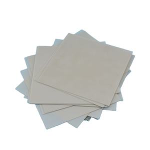
( Aluminum Nitride Ceramic Substrates)
2.1 Powder Synthesis and Sintering Methods
Producing high-performance AlN substratums begins with the synthesis of ultra-fine, high-purity powder, frequently attained through reactions such as Al ₂ O TWO + 3C + N ₂ → 2AlN + 3CO (carbothermal decrease) or direct nitridation of light weight aluminum metal: 2Al + N TWO → 2AlN.
The resulting powder must be very carefully grated and doped with sintering help like Y TWO O FIVE, CaO, or uncommon earth oxides to advertise densification at temperature levels in between 1700 ° C and 1900 ° C under nitrogen atmosphere.
These ingredients create transient liquid phases that improve grain limit diffusion, enabling full densification (> 99% academic density) while reducing oxygen contamination.
Post-sintering annealing in carbon-rich settings can additionally minimize oxygen web content by removing intergranular oxides, consequently bring back peak thermal conductivity.
Attaining uniform microstructure with regulated grain dimension is essential to balance mechanical toughness, thermal efficiency, and manufacturability.
2.2 Substrate Shaping and Metallization
Once sintered, AlN ceramics are precision-ground and lapped to meet tight dimensional resistances required for electronic product packaging, usually down to micrometer-level flatness.
Through-hole boring, laser cutting, and surface patterning make it possible for combination into multilayer packages and crossbreed circuits.
An essential action in substratum fabrication is metallization– the application of conductive layers (normally tungsten, molybdenum, or copper) by means of procedures such as thick-film printing, thin-film sputtering, or direct bonding of copper (DBC).
For DBC, copper aluminum foils are adhered to AlN surfaces at raised temperatures in a regulated atmosphere, forming a solid user interface suitable for high-current applications.
Alternative techniques like active metal brazing (AMB) use titanium-containing solders to enhance bond and thermal tiredness resistance, particularly under repeated power biking.
Appropriate interfacial design makes sure reduced thermal resistance and high mechanical reliability in operating gadgets.
3. Efficiency Advantages in Electronic Equipment
3.1 Thermal Administration in Power Electronics
AlN substrates excel in managing heat created by high-power semiconductor gadgets such as IGBTs, MOSFETs, and RF amplifiers utilized in electric lorries, renewable resource inverters, and telecommunications infrastructure.
Efficient warm removal prevents local hotspots, decreases thermal stress, and extends tool lifetime by minimizing electromigration and delamination risks.
Compared to conventional Al two O three substratums, AlN enables smaller sized bundle dimensions and greater power densities because of its superior thermal conductivity, allowing designers to push efficiency boundaries without compromising dependability.
In LED illumination and laser diodes, where junction temperature level directly affects performance and color security, AlN substratums dramatically boost luminous output and functional life expectancy.
Its coefficient of thermal growth (CTE ≈ 4.5 ppm/K) additionally carefully matches that of silicon (3.5– 4 ppm/K) and gallium nitride (GaN, ~ 5.6 ppm/K), minimizing thermo-mechanical tension throughout thermal cycling.
3.2 Electrical and Mechanical Integrity
Beyond thermal performance, AlN uses low dielectric loss (tan δ < 0.0005) and steady permittivity (εᵣ ≈ 8.9) throughout a broad frequency variety, making it perfect for high-frequency microwave and millimeter-wave circuits.
Its hermetic nature avoids dampness access, removing deterioration risks in humid environments– an essential advantage over natural substrates.
Mechanically, AlN possesses high flexural toughness (300– 400 MPa) and firmness (HV ≈ 1200), ensuring resilience during handling, setting up, and field operation.
These features jointly add to enhanced system reliability, minimized failure prices, and lower overall cost of ownership in mission-critical applications.
4. Applications and Future Technological Frontiers
4.1 Industrial, Automotive, and Defense Systems
AlN ceramic substrates are currently typical in sophisticated power modules for industrial electric motor drives, wind and solar inverters, and onboard battery chargers in electric and hybrid vehicles.
In aerospace and protection, they sustain radar systems, digital warfare units, and satellite interactions, where efficiency under extreme problems is non-negotiable.
Medical imaging tools, consisting of X-ray generators and MRI systems, additionally gain from AlN’s radiation resistance and signal stability.
As electrification patterns accelerate across transportation and energy sectors, demand for AlN substratums continues to grow, driven by the requirement for compact, efficient, and dependable power electronic devices.
4.2 Emerging Assimilation and Lasting Development
Future advancements concentrate on integrating AlN right into three-dimensional packaging styles, ingrained passive elements, and heterogeneous assimilation platforms combining Si, SiC, and GaN tools.
Research right into nanostructured AlN movies and single-crystal substratums aims to additional increase thermal conductivity towards academic restrictions (> 300 W/(m · K)) for next-generation quantum and optoelectronic gadgets.
Efforts to lower manufacturing prices via scalable powder synthesis, additive manufacturing of intricate ceramic structures, and recycling of scrap AlN are getting momentum to improve sustainability.
Additionally, modeling tools making use of limited element analysis (FEA) and machine learning are being employed to enhance substrate layout for specific thermal and electric lots.
To conclude, aluminum nitride ceramic substrates represent a cornerstone innovation in modern-day electronics, distinctively connecting the space in between electric insulation and extraordinary thermal conduction.
Their function in allowing high-efficiency, high-reliability power systems emphasizes their tactical relevance in the recurring advancement of electronic and power technologies.
5. Vendor
Advanced Ceramics founded on October 17, 2012, is a high-tech enterprise committed to the research and development, production, processing, sales and technical services of ceramic relative materials and products. Our products includes but not limited to Boron Carbide Ceramic Products, Boron Nitride Ceramic Products, Silicon Carbide Ceramic Products, Silicon Nitride Ceramic Products, Zirconium Dioxide Ceramic Products, etc. If you are interested, please feel free to contact us.
Tags: Aluminum Nitride Ceramic Substrates, aluminum nitride ceramic, aln aluminium nitride
All articles and pictures are from the Internet. If there are any copyright issues, please contact us in time to delete.
Inquiry us