1. Fundamental Features and Nanoscale Behavior of Silicon at the Submicron Frontier
1.1 Quantum Confinement and Electronic Framework Change
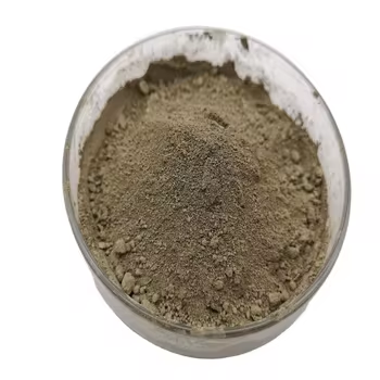
(Nano-Silicon Powder)
Nano-silicon powder, made up of silicon fragments with characteristic dimensions listed below 100 nanometers, represents a paradigm shift from mass silicon in both physical habits and functional energy.
While mass silicon is an indirect bandgap semiconductor with a bandgap of roughly 1.12 eV, nano-sizing generates quantum confinement results that essentially alter its electronic and optical homes.
When the bit size strategies or falls below the exciton Bohr radius of silicon (~ 5 nm), cost providers end up being spatially restricted, leading to a widening of the bandgap and the development of noticeable photoluminescence– a sensation lacking in macroscopic silicon.
This size-dependent tunability enables nano-silicon to produce light throughout the visible range, making it a promising candidate for silicon-based optoelectronics, where standard silicon fails because of its inadequate radiative recombination performance.
Additionally, the increased surface-to-volume ratio at the nanoscale enhances surface-related phenomena, including chemical reactivity, catalytic activity, and communication with electromagnetic fields.
These quantum results are not merely scholastic curiosities but develop the structure for next-generation applications in power, picking up, and biomedicine.
1.2 Morphological Diversity and Surface Area Chemistry
Nano-silicon powder can be synthesized in numerous morphologies, including round nanoparticles, nanowires, permeable nanostructures, and crystalline quantum dots, each offering distinctive benefits depending upon the target application.
Crystalline nano-silicon generally keeps the ruby cubic structure of bulk silicon however displays a higher density of surface problems and dangling bonds, which need to be passivated to maintain the product.
Surface area functionalization– typically attained via oxidation, hydrosilylation, or ligand attachment– plays an important role in figuring out colloidal security, dispersibility, and compatibility with matrices in composites or organic settings.
For example, hydrogen-terminated nano-silicon shows high reactivity and is vulnerable to oxidation in air, whereas alkyl- or polyethylene glycol (PEG)-coated fragments show boosted security and biocompatibility for biomedical use.
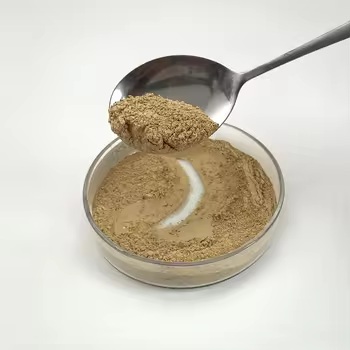
( Nano-Silicon Powder)
The visibility of an indigenous oxide layer (SiOₓ) on the bit surface, even in marginal amounts, dramatically influences electrical conductivity, lithium-ion diffusion kinetics, and interfacial reactions, specifically in battery applications.
Understanding and controlling surface chemistry is for that reason important for harnessing the full capacity of nano-silicon in practical systems.
2. Synthesis Techniques and Scalable Manufacture Techniques
2.1 Top-Down Techniques: Milling, Etching, and Laser Ablation
The production of nano-silicon powder can be generally classified into top-down and bottom-up methods, each with distinctive scalability, purity, and morphological control characteristics.
Top-down strategies include the physical or chemical reduction of bulk silicon right into nanoscale pieces.
High-energy sphere milling is a commonly utilized commercial method, where silicon pieces go through extreme mechanical grinding in inert environments, causing micron- to nano-sized powders.
While affordable and scalable, this technique often presents crystal defects, contamination from milling media, and wide fragment dimension circulations, requiring post-processing filtration.
Magnesiothermic reduction of silica (SiO ₂) followed by acid leaching is another scalable course, specifically when using natural or waste-derived silica resources such as rice husks or diatoms, providing a lasting pathway to nano-silicon.
Laser ablation and reactive plasma etching are more specific top-down techniques, capable of generating high-purity nano-silicon with controlled crystallinity, however at higher price and lower throughput.
2.2 Bottom-Up Techniques: Gas-Phase and Solution-Phase Development
Bottom-up synthesis permits higher control over fragment dimension, shape, and crystallinity by building nanostructures atom by atom.
Chemical vapor deposition (CVD) and plasma-enhanced CVD (PECVD) make it possible for the growth of nano-silicon from aeriform forerunners such as silane (SiH FOUR) or disilane (Si ₂ H ₆), with parameters like temperature level, stress, and gas circulation determining nucleation and development kinetics.
These techniques are specifically effective for generating silicon nanocrystals embedded in dielectric matrices for optoelectronic tools.
Solution-phase synthesis, consisting of colloidal routes using organosilicon compounds, enables the production of monodisperse silicon quantum dots with tunable emission wavelengths.
Thermal decay of silane in high-boiling solvents or supercritical liquid synthesis also generates high-quality nano-silicon with narrow dimension circulations, ideal for biomedical labeling and imaging.
While bottom-up approaches typically generate premium material quality, they face difficulties in large-scale production and cost-efficiency, demanding recurring research study right into hybrid and continuous-flow processes.
3. Energy Applications: Reinventing Lithium-Ion and Beyond-Lithium Batteries
3.1 Function in High-Capacity Anodes for Lithium-Ion Batteries
One of one of the most transformative applications of nano-silicon powder depends on power storage space, particularly as an anode product in lithium-ion batteries (LIBs).
Silicon supplies a theoretical specific capability of ~ 3579 mAh/g based upon the development of Li ₁₅ Si Four, which is nearly 10 times greater than that of conventional graphite (372 mAh/g).
Nonetheless, the large volume growth (~ 300%) throughout lithiation triggers fragment pulverization, loss of electrical get in touch with, and continuous strong electrolyte interphase (SEI) development, causing quick capacity fade.
Nanostructuring mitigates these concerns by reducing lithium diffusion paths, suiting stress better, and minimizing fracture likelihood.
Nano-silicon in the type of nanoparticles, porous structures, or yolk-shell frameworks enables relatively easy to fix biking with enhanced Coulombic performance and cycle life.
Commercial battery technologies currently incorporate nano-silicon blends (e.g., silicon-carbon composites) in anodes to improve energy density in customer electronics, electric cars, and grid storage space systems.
3.2 Prospective in Sodium-Ion, Potassium-Ion, and Solid-State Batteries
Past lithium-ion systems, nano-silicon is being explored in arising battery chemistries.
While silicon is much less reactive with salt than lithium, nano-sizing enhances kinetics and makes it possible for restricted Na ⁺ insertion, making it a prospect for sodium-ion battery anodes, specifically when alloyed or composited with tin or antimony.
In solid-state batteries, where mechanical security at electrode-electrolyte interfaces is critical, nano-silicon’s capability to go through plastic deformation at small ranges minimizes interfacial anxiety and boosts contact maintenance.
Additionally, its compatibility with sulfide- and oxide-based strong electrolytes opens up opportunities for much safer, higher-energy-density storage remedies.
Research continues to maximize user interface engineering and prelithiation methods to maximize the longevity and performance of nano-silicon-based electrodes.
4. Emerging Frontiers in Photonics, Biomedicine, and Compound Products
4.1 Applications in Optoelectronics and Quantum Source Of Light
The photoluminescent buildings of nano-silicon have rejuvenated initiatives to create silicon-based light-emitting gadgets, a long-lasting challenge in integrated photonics.
Unlike bulk silicon, nano-silicon quantum dots can show effective, tunable photoluminescence in the visible to near-infrared variety, allowing on-chip source of lights suitable with complementary metal-oxide-semiconductor (CMOS) technology.
These nanomaterials are being integrated into light-emitting diodes (LEDs), photodetectors, and waveguide-coupled emitters for optical interconnects and picking up applications.
Furthermore, surface-engineered nano-silicon exhibits single-photon discharge under specific flaw setups, positioning it as a possible platform for quantum information processing and safe interaction.
4.2 Biomedical and Environmental Applications
In biomedicine, nano-silicon powder is obtaining attention as a biocompatible, eco-friendly, and non-toxic option to heavy-metal-based quantum dots for bioimaging and medicine distribution.
Surface-functionalized nano-silicon particles can be created to target specific cells, release healing agents in reaction to pH or enzymes, and give real-time fluorescence monitoring.
Their destruction right into silicic acid (Si(OH)₄), a naturally taking place and excretable substance, minimizes long-term toxicity issues.
Additionally, nano-silicon is being examined for ecological remediation, such as photocatalytic degradation of toxins under noticeable light or as a lowering representative in water therapy processes.
In composite materials, nano-silicon improves mechanical strength, thermal stability, and use resistance when incorporated into steels, ceramics, or polymers, particularly in aerospace and auto elements.
In conclusion, nano-silicon powder stands at the crossway of essential nanoscience and industrial advancement.
Its distinct combination of quantum results, high reactivity, and flexibility throughout power, electronics, and life sciences emphasizes its duty as a key enabler of next-generation technologies.
As synthesis techniques breakthrough and combination obstacles are overcome, nano-silicon will continue to drive development towards higher-performance, sustainable, and multifunctional material systems.
5. Provider
TRUNNANO is a supplier of Spherical Tungsten Powder with over 12 years of experience in nano-building energy conservation and nanotechnology development. It accepts payment via Credit Card, T/T, West Union and Paypal. Trunnano will ship the goods to customers overseas through FedEx, DHL, by air, or by sea. If you want to know more about Spherical Tungsten Powder, please feel free to contact us and send an inquiry(sales5@nanotrun.com).
Tags: Nano-Silicon Powder, Silicon Powder, Silicon
All articles and pictures are from the Internet. If there are any copyright issues, please contact us in time to delete.
Inquiry us