1. Product Fundamentals and Architectural Features of Alumina Ceramics
1.1 Crystallographic and Compositional Basis of α-Alumina
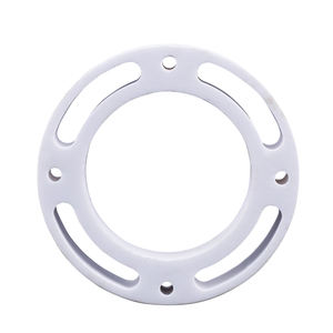
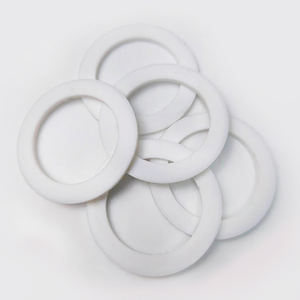
(Alumina Ceramic Substrates)
Alumina ceramic substrates, mainly made up of aluminum oxide (Al ₂ O SIX), serve as the foundation of modern electronic product packaging because of their extraordinary equilibrium of electrical insulation, thermal security, mechanical strength, and manufacturability.
One of the most thermodynamically stable phase of alumina at heats is diamond, or α-Al ₂ O SIX, which crystallizes in a hexagonal close-packed oxygen latticework with light weight aluminum ions inhabiting two-thirds of the octahedral interstitial websites.
This dense atomic arrangement imparts high solidity (Mohs 9), excellent wear resistance, and strong chemical inertness, making α-alumina appropriate for rough operating settings.
Commercial substrates normally consist of 90– 99.8% Al Two O TWO, with small enhancements of silica (SiO TWO), magnesia (MgO), or unusual planet oxides utilized as sintering aids to advertise densification and control grain development during high-temperature processing.
Higher pureness qualities (e.g., 99.5% and above) show remarkable electric resistivity and thermal conductivity, while lower pureness variants (90– 96%) use affordable options for much less demanding applications.
1.2 Microstructure and Problem Engineering for Electronic Reliability
The efficiency of alumina substrates in digital systems is critically dependent on microstructural uniformity and issue reduction.
A fine, equiaxed grain framework– typically ranging from 1 to 10 micrometers– makes certain mechanical stability and minimizes the likelihood of fracture breeding under thermal or mechanical tension.
Porosity, specifically interconnected or surface-connected pores, need to be lessened as it weakens both mechanical stamina and dielectric efficiency.
Advanced processing strategies such as tape casting, isostatic pushing, and controlled sintering in air or regulated ambiences allow the production of substrates with near-theoretical thickness (> 99.5%) and surface area roughness listed below 0.5 µm, necessary for thin-film metallization and cable bonding.
Additionally, contamination segregation at grain boundaries can cause leak currents or electrochemical movement under bias, demanding strict control over basic material pureness and sintering problems to make certain lasting reliability in damp or high-voltage environments.
2. Manufacturing Processes and Substratum Fabrication Technologies
( Alumina Ceramic Substrates)
2.1 Tape Casting and Environment-friendly Body Processing
The production of alumina ceramic substrates begins with the prep work of an extremely dispersed slurry containing submicron Al ₂ O four powder, natural binders, plasticizers, dispersants, and solvents.
This slurry is processed by means of tape spreading– a constant method where the suspension is topped a moving carrier film utilizing an accuracy doctor blade to attain uniform thickness, normally between 0.1 mm and 1.0 mm.
After solvent dissipation, the resulting “eco-friendly tape” is adaptable and can be punched, drilled, or laser-cut to develop via holes for vertical affiliations.
Multiple layers might be laminated to produce multilayer substratums for complicated circuit assimilation, although the majority of commercial applications make use of single-layer configurations as a result of cost and thermal expansion considerations.
The environment-friendly tapes are then carefully debound to remove natural ingredients via managed thermal decomposition before final sintering.
2.2 Sintering and Metallization for Circuit Assimilation
Sintering is performed in air at temperature levels in between 1550 ° C and 1650 ° C, where solid-state diffusion drives pore elimination and grain coarsening to achieve complete densification.
The linear shrinkage during sintering– commonly 15– 20%– must be specifically anticipated and compensated for in the style of eco-friendly tapes to make certain dimensional precision of the final substratum.
Adhering to sintering, metallization is related to form conductive traces, pads, and vias.
2 primary approaches control: thick-film printing and thin-film deposition.
In thick-film innovation, pastes having metal powders (e.g., tungsten, molybdenum, or silver-palladium alloys) are screen-printed onto the substratum and co-fired in a lowering atmosphere to form durable, high-adhesion conductors.
For high-density or high-frequency applications, thin-film procedures such as sputtering or dissipation are made use of to deposit bond layers (e.g., titanium or chromium) followed by copper or gold, allowing sub-micron patterning via photolithography.
Vias are full of conductive pastes and fired to develop electrical interconnections between layers in multilayer designs.
3. Functional Characteristics and Efficiency Metrics in Electronic Systems
3.1 Thermal and Electric Actions Under Functional Tension
Alumina substrates are valued for their desirable combination of modest thermal conductivity (20– 35 W/m · K for 96– 99.8% Al Two O FOUR), which enables effective warm dissipation from power tools, and high quantity resistivity (> 10 ¹⁴ Ω · cm), making sure very little leak current.
Their dielectric consistent (εᵣ ≈ 9– 10 at 1 MHz) is stable over a broad temperature level and frequency range, making them suitable for high-frequency circuits as much as several ghzs, although lower-κ products like light weight aluminum nitride are preferred for mm-wave applications.
The coefficient of thermal development (CTE) of alumina (~ 6.8– 7.2 ppm/K) is sensibly well-matched to that of silicon (~ 3 ppm/K) and certain packaging alloys, lowering thermo-mechanical stress and anxiety throughout tool operation and thermal biking.
However, the CTE mismatch with silicon continues to be a problem in flip-chip and direct die-attach setups, usually calling for compliant interposers or underfill products to minimize tiredness failure.
3.2 Mechanical Robustness and Environmental Resilience
Mechanically, alumina substratums show high flexural stamina (300– 400 MPa) and outstanding dimensional stability under load, allowing their usage in ruggedized electronics for aerospace, automotive, and industrial control systems.
They are resistant to resonance, shock, and creep at elevated temperature levels, keeping structural stability up to 1500 ° C in inert atmospheres.
In moist atmospheres, high-purity alumina shows minimal dampness absorption and outstanding resistance to ion migration, making certain lasting reliability in outdoor and high-humidity applications.
Surface hardness also shields against mechanical damages throughout handling and setting up, although treatment needs to be taken to prevent edge chipping due to intrinsic brittleness.
4. Industrial Applications and Technological Impact Throughout Sectors
4.1 Power Electronics, RF Modules, and Automotive Equipments
Alumina ceramic substrates are ubiquitous in power digital modules, including protected gate bipolar transistors (IGBTs), MOSFETs, and rectifiers, where they provide electric seclusion while promoting warm transfer to warmth sinks.
In superhigh frequency (RF) and microwave circuits, they serve as provider platforms for crossbreed integrated circuits (HICs), surface acoustic wave (SAW) filters, and antenna feed networks because of their steady dielectric residential or commercial properties and reduced loss tangent.
In the auto sector, alumina substrates are utilized in engine control units (ECUs), sensor bundles, and electric lorry (EV) power converters, where they endure heats, thermal biking, and direct exposure to destructive liquids.
Their integrity under harsh conditions makes them important for safety-critical systems such as anti-lock braking (ABS) and progressed vehicle driver assistance systems (ADAS).
4.2 Clinical Gadgets, Aerospace, and Emerging Micro-Electro-Mechanical Systems
Beyond consumer and commercial electronic devices, alumina substrates are employed in implantable medical tools such as pacemakers and neurostimulators, where hermetic securing and biocompatibility are paramount.
In aerospace and defense, they are made use of in avionics, radar systems, and satellite interaction components as a result of their radiation resistance and security in vacuum settings.
Additionally, alumina is significantly made use of as a structural and protecting platform in micro-electro-mechanical systems (MEMS), consisting of pressure sensors, accelerometers, and microfluidic gadgets, where its chemical inertness and compatibility with thin-film processing are useful.
As digital systems continue to require greater power thickness, miniaturization, and dependability under extreme conditions, alumina ceramic substrates stay a keystone material, linking the space in between performance, cost, and manufacturability in sophisticated digital product packaging.
5. Vendor
Alumina Technology Co., Ltd focus on the research and development, production and sales of aluminum oxide powder, aluminum oxide products, aluminum oxide crucible, etc., serving the electronics, ceramics, chemical and other industries. Since its establishment in 2005, the company has been committed to providing customers with the best products and services. If you are looking for high quality porous alumina, please feel free to contact us. (nanotrun@yahoo.com)
Tags: Alumina Ceramic Substrates, Alumina Ceramics, alumina
All articles and pictures are from the Internet. If there are any copyright issues, please contact us in time to delete.
Inquiry us